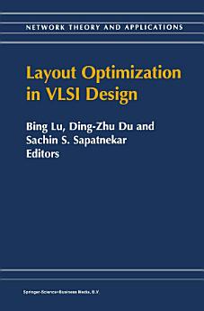
Layout Optimization in VLSI Design
Bing Lu · Ding-Zhu Du · S. Sapatnekar
2013年6月 · Network Theory and Applications 8 巻 · Springer Science & Business Media
2.0star
4 件のレビューreport
電子書籍
288
ページ
report評価とレビューは確認済みではありません 詳細
この電子書籍について
Introduction The exponential scaling of feature sizes in semiconductor technologies has side-effects on layout optimization, related to effects such as inter connect delay, noise and crosstalk, signal integrity, parasitics effects, and power dissipation, that invalidate the assumptions that form the basis of previous design methodologies and tools. This book is intended to sample the most important, contemporary, and advanced layout opti mization problems emerging with the advent of very deep submicron technologies in semiconductor processing. We hope that it will stimulate more people to perform research that leads to advances in the design and development of more efficient, effective, and elegant algorithms and design tools. Organization of the Book The book is organized as follows. A multi-stage simulated annealing algorithm that integrates floorplanning and interconnect planning is pre sented in Chapter 1. To reduce the run time, different interconnect plan ning approaches are applied in different ranges of temperatures. Chapter 2 introduces a new design methodology - the interconnect-centric design methodology and its centerpiece, interconnect planning, which consists of physical hierarchy generation, floorplanning with interconnect planning, and interconnect architecture planning. Chapter 3 investigates a net-cut minimization based placement tool, Dragon, which integrates the state of the art partitioning and placement techniques.
評価とレビュー
2.0
4 件のレビュー
この電子書籍を評価する
ご感想をお聞かせください。
読書情報
スマートフォンとタブレット
Android や iPad / iPhone 用の Google Play ブックス アプリをインストールしてください。このアプリがアカウントと自動的に同期するため、どこでもオンラインやオフラインで読むことができます。
ノートパソコンとデスクトップ パソコン
Google Play で購入したオーディブックは、パソコンのウェブブラウザで再生できます。
電子書籍リーダーなどのデバイス
Kobo 電子書籍リーダーなどの E Ink デバイスで読むには、ファイルをダウンロードしてデバイスに転送する必要があります。サポートされている電子書籍リーダーにファイルを転送する方法について詳しくは、ヘルプセンターをご覧ください。